ASIC Implementations
X-HEEP is designed to be a simple yet extensible RISC-V microcontroller, perfect for tightly integrating your own custom accelerators within an ASIC. This approach lets you concentrate on accelerator design, while inheriting a complete RISC-V system, including peripherals, software stacks, FPGA support, and application examples — significantly simplifying hardware integration and application deployment.
Building your “chip” around a full RISC-V microcontroller, rather than just the accelerator, makes testing and demonstrations much easier. Having a CPU to manage peripherals and handle parts of the application outside the accelerator’s scope enables the deployment of complete, end-to-end applications.
That’s why we use X-HEEP for testing our accelerators and other custom hardware, and we highly recommend it to you!
To create an ASIC with X-HEEP and your custom accelerator, you’ll need to add a pad ring and pad controller (optionally including a frequency-locked loop, or FLL) and integrate your accelerator with X-HEEP.
X-HEEP is freely available under the Solderpad license, empowering anyone to create their own chips.
Following you find ASIC implementations that uses X-HEEP.
HEEPocrates
HEEPocrates is the first silicon implementation of X-HEEP made by us, i.e. the ESL Lab of EPFL.
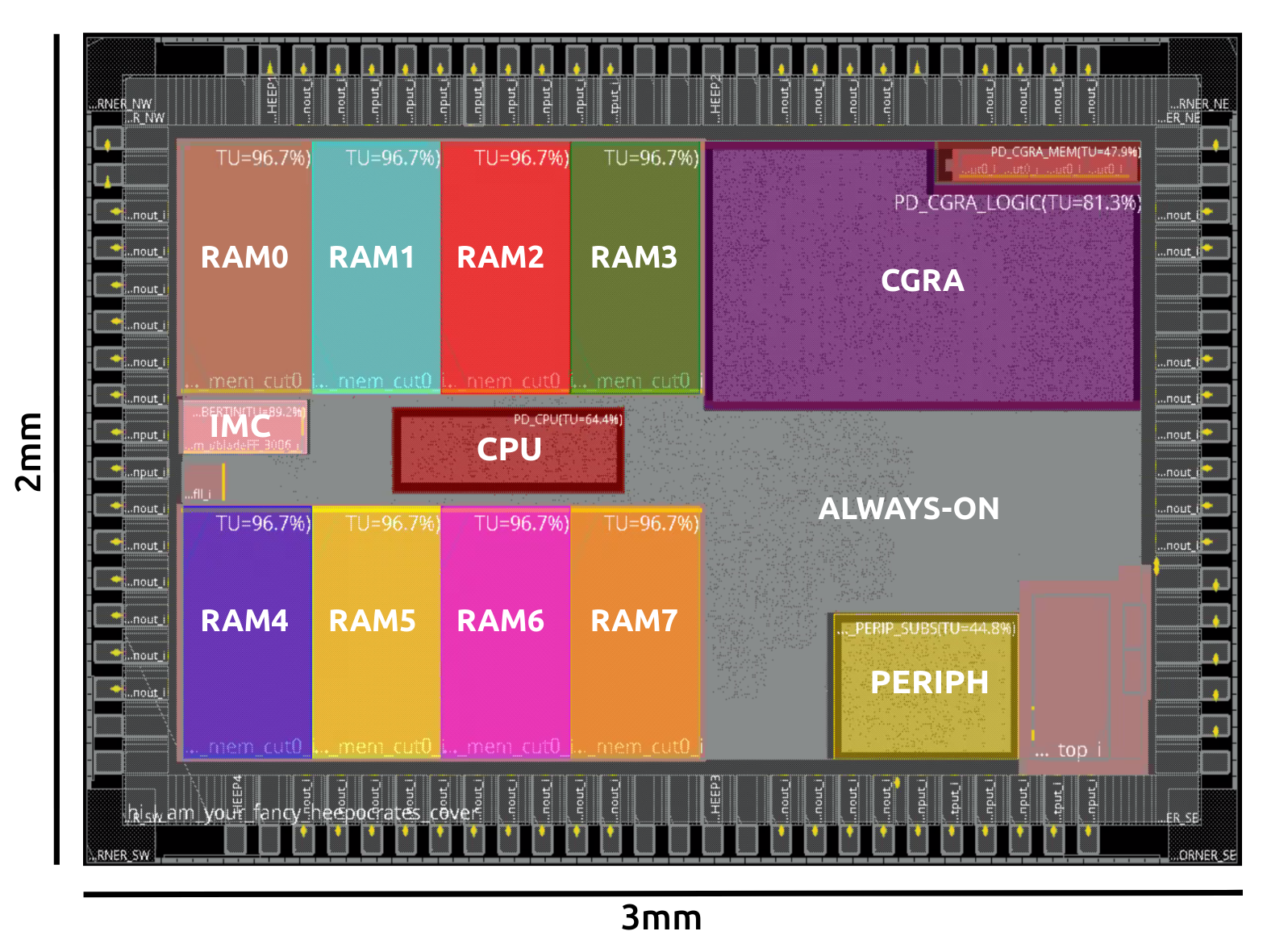
Figure 1: HEEPocrates Test Chip layout in TSMC 65nm LP
HEEPocrates, taped out in November 2022, is based on X-HEEP and features the CV32E2 CPU, 256KB of memory (organized into eight 32KB banks), and peripherals including a DMA, two SPI interfaces, an I2C interface, GPIOs, a UART, and JTAG.
It has been used to integrate the OpenEdgeCGRA and the Blade in-memory-computing macro.
Clock generation is handled by a frequency-locked loop (FLL) from the PULP project.
Implemented in TSMC 65nm LP CMOS technology using low-voltage threshold (LVT) cells, HEEPocrates targets ultra-low-power healthcare applications, which often have diverse data size, performance, and energy requirements. To address this, HEEPocrates employs fine-grained power domains, enabling precise control over which components are active and which are powered off.
The CPU itself resides in its own power domain and is typically power-gated during long acquisition periods. After the SPI-DMA subsystem completes writing data to memory, an interrupt wakes the core. Furthermore, unused memory banks are selectively powered off via dedicated power-gating cells, based on the data and instructions required. Finally, less frequently used peripherals and the CGRA accelerators also have their own power domains, allowing them to be kept off when not in use.
For more information about the HEEPocrates, check this paper, and if you want to cite it, you can use:
@misc{machetti2024xheep,
      title={X-HEEP: An Open-Source, Configurable and Extendible RISC-V Microcontroller for the Exploration of Ultra-Low-Power Edge Accelerators},
      author={Simone Machetti and Pasquale Davide Schiavone and Thomas Christoph Müller and Miguel Peón-Quirós and David Atienza},
      year={2024},
      eprint={2401.05548},
      archivePrefix={arXiv},
      primaryClass={cs.AR}
}
Other resources that leverages HEEPocrates (silicon implementation, FPGA, or simulation results) are:
HEEPnosis
HEEPnosis is the second silicon implementation of X-HEEP, made by a collaboration between the ESL lab and the
TCL lab of EPFL.
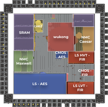
Figure 2: HEEPnosis Test Chip layout in GF 22nm FDX
HEEPnosis, taped out in February 2025, utilizes X-HEEP configured with the CV32E2 CPU, 128KB of memory split into four 32KB banks: two contiguous and two interleaved. Peripherals include two DMAs, an SPI interface, GPIOs, a UART, and JTAG.
This chip integrates the Near-Memory macros Caesar and Maxwell, as well as the Wukong peripheral. It also incorporates several test IPs implemented using various logic-suppression styles and transistor flavors. An FLL from the PULP project provides clock generation.
HEEPnosis is implemented in GF 22nm FDX technology using a mix of LVT, HVT, and UHVT cells. Its primary purpose is to validate the functionality and efficiency of full-custom blocks designed with logic suppression, as well as to verify the performance and functionality of the integrated near-memory macros.
This chip has been sponsored by SwissChips.
There are no references yet about this chip as it hasn’t been tested yet.
X-TRELA
X-TRELA is the third silicon implementation of X-HEEP, developed by the CEI lab of the Universidad Politécnica de Madrid (UPM), Spain.

Figure 3: X-TRELA Test Chip layout in TSMC 65nm LP
The chip was taped out in February 2025. The chosen X-HEEP configuration for this SoC includes a CV32E40P CPU, an NtoM bus topology, and 256 KB of memory distributed across four contiguous and four interleaved banks of 32 KB each. Peripherals include a DMA, SPI interfaces, an I2C interface, GPIOs, a UART, and JTAG. X-TRELA integrates a STReaming ELAstic Coarse-Grained Reconfigurable Architecture (CGRA) of 32-bit 4x4 Processing Elements, supporting dataflow data- and control-oriented applications. For more information about this hardware accelerator, check this preprint paper.
The design uses LVT cells, slim digital IOs, and CUP bondpads, and memory macros sourced from ARM. This is the first tape out of CEI-UPM, employing a single power domain to simplify the ASIC flow.
This chip has been funded by the A-IQ Ready project, supported by the Spanish Government MICIU/AEI 10.13039/501100011033 (PCI2022-135077-2) and the European Union NextGenerationEU/PRTR (101096658).
HEEPidermis
HEEPidermis is the first X-HEEP MCU extended with an analog front end. It was built as a collaboration of the Embedded Systems Laboratory (ESL) of EPFL with Universidad Católica del Uruguay (UCU) and Politecnico di Torino.
It was designed to record Galvanic Skin Response (GSR), for which it includes two 8-bit current Digital-to-Analog Converters (iDACs) and two digitization channels with a VCO-based ADC, which can be used independently or as pseudo differential. The integrated DMA allows the autonomous operation of iDACs and ADCs. Additionally, the DMA can filter data before it is stored in memory by diverting it into a Level-Crossing stream accelerator.
HEEPidermis can be used as a powerful ADC with embedded feature extraction by reading data through its SPI slave interface. It can also control external ADCs for more versatile measurements, both trough SPI and through a dedicated ΔΣ input where data can be decimated.

Figure 4: HEEPidermis Test Chip layout in TSMC 65nm LP
This chip has been sponsored by SwissChips.
X-EROS
X‑EROS is a silicon tape‑out of the X‑HEEP design carried out by the CEI lab at the Universidad Politécnica de Madrid (UPM), Spain.

Figure 3: X-EROS Test Chip layout in TSMC 65nm LP
The chip was taped out in June 2025. The chosen X-HEEP configuration for this SoC includes a CV32E40P CPU, an NtoM bus topology and four 128KB contiguous banks of 32 KB each. Peripherals include a DMA, SPI interfaces, an I2C interface, GPIOs, a UART, and JTAG.
X-EROS integrates an Extensible Reliable Offloading Solution (EROS), featuring three CV32E20 CPU capable of operating in both safety and non‑safety modes and two 32 KB memory banks for instruction and data respectively. It is intended to serve as a safety‑critical accelerator island for mixed‑critical applications.
For more information about this safety island accelerator, check this paper.
The design uses LVT cells, slim digital IOs, and CUP bondpads, and memory macros sourced from ARM. This is the second tape-out of CEI-UPM, employing a single power domain to simplify the ASIC flow.
This chip has been sponsored by Talent2Concept (PDC2023-145865)
HEEPatia
HEEPatia is the first silicon implementation of X-HEEP taped out in the TSMC 16nm technology. It was built as part of a collaboration between the EPFL Embedded Systems Laboratory and Telecommunication Circuits Laboratory, as well as Politecnico di Torino.

Figure 4: HEEPatia Test Chip layout in TSMC 16nm
HEEPatia, taped out in July 2025, utilizes a dual-core X-HEEP implementation configured with the CV32E40P and CV32E40PX CPUs, the latter of which is extended with the Coprosit coprocessing unit for posit arithmetic. HEEPatia contains a total of 608 kB of memory, including 352 kB of SRAM among the MCU and IPs, as well as 256 kB of Gain-Cell Random Access Memory.
In addition to the novel coprocessor and memory units, HEEPatia contains various heterogeneous accelerator architectures to improve the performance and decrease the energy consumption of different edge-AI workloads. Namely, it integrates two instances of near-memory computing Carus with the DomaIn-specific System-technology CO-design (DISCO) CGRA, an IP based on the VWR2A architecture.
HEEPatia is implemented using a mixture of LVT and SVT cells. Its purposes are to serve as a research platform used for comparing various hardware IPs in terms of PPA trade-offs, and to use a combination of the aforementioned IPs to execute state-of-the-art edge-AI applications.
This chip has been sponsored by SwissChips.
polHEEPo
polHEEPo is the first silicon tape‑out of the X‑HEEP design carried out by the VLSI lab at the Politecnico di Torino, Italy.

Figure 5: polHEEPo Test Chip layout in TSMC 65nm LP
The chip was taped out in October 2025. The chosen X-HEEP configuration for this SoC includes a CV32E40P CPU, an NtoM bus topology and ten interleaved banks of 32 KB each for a total of 320 KB of on-chip memory. Peripherals include a 4 channel DMA, configured to have 4 maasters on the bus, SPI interfaces, an I2C interface, GPIOs, a UART, and JTAG.
polHEEPo integrates different accelerators to target many applications, from edge AI and ML to postquantum cryptography. These include KECCAK, ASCON, and ROGUE, targeting post-quantum cryptography, lightweight cryptography, and AI/ML workloads. There is also PUFFo, which is a hardware Physically Unclonable Function (PUF) module, enabling on-chip generation of unique and tamper-resistant cryptographic keys.
The design uses LVT cells, slim digital IOs, and CUP bondpads, and memory macros sourced from TSMC.
This chip has been sponsored by project SERICS (PE00000014) under the MUR National Recovery and Resilience Plan funded by the European Union – NextGenerationEU with the collaboration of Chips-IT foundation.
HEEPokranios
HEEPokranios is a neural recording SoC powered by an X-HEEP MCU. It was built as a collaboration of the Embedded Systems Laboratory (ESL) of EPFL with Universidad Católica del Uruguay (UCU) and Imperial College London.
It was designed to record intracortical EEG through a diverse set of front-ends spanning from high-resolution Delta-Sigma modulators to spiking band power feature extraction and event-based ADCs.
HEEPokranios can be used standalone thanks to its Wireless Power and Data Transfer (WPDT) block, which can provide the SoC with the power and bandwidth to acquire and stream several channels simultaneously. All needed references and regulators are integrated on-chip.
Five shanks at the bottom of the chip will enable in-vitro recordings of up to 4 indepedent channels. Additionally, the first shank includes a current DAC to monitor electrode-tissue impedance.

HEEPokranios SoC top-level layout in TSMC 65nm LP
This chip has been sponsored by SwissChips.