Pad Configuration
The pads of the design are configured using a Python configuration file, which is then read by mcu-gen and template files to generate the pad ring RTL and back-end pad IO of the design (not included in this repo).
Overview
The pad configuration system allows you to define:
Pins (Signals): The logical signals in your design (e.g.,
clk,gpio_0,uart_tx). Optionally, also analog and supply signals.Pin-to-Pad Mapping: How pins are assigned to physical pads on each side of the chip, including multiplexing (assign multiple pins to the same pad, or a single pin to multiple pads).
(Optional) Floorplan: Physical layout of the die and location of the pads.
The configuration is done through a Python config(xheep: XHeep) function that accepts an XHeep object as its only argument and returns a PadRing object. This approach provides flexibility and programmatic generation of pad configurations and allwos the pad generation to depend on the current X-HEEP configuration passed as an argument. The default pad configuration file can be found in configs/pad_cfg.py.
The default call to mcu-gen uses the default pad configuration, but you can specify a custom pad configuration file using the PADS_CFG variable:
make mcu-gen PADS_CFG=configs/my_pad_cfg.py
Please refer to the diagram in the Visualization section below for clarification.
Pin Types
Pins represent the signals in your design. Different pin types are available depending on the signal direction and characteristics. The digital pin types include:
from pads.pin import Input, Output, Inout

# Input pin
clk_pin = Input("clk")

# Output pin
tx_pin = Output("uart_tx")

# Bidirectional pin
gpio_pin = Inout("gpio_0")
Other pin types can be defined, including for analog signals and power supply. For this, see the X-pert Zone section below.
Pin Attributes
Pins can have additional attributes that modify their behavior:
The
moduleattribute is an optional string that specifies which module in the design the pin is connected to. Does it belong to an external peripheral? Does it stay in the top-level module? You can define your own names. By default, it is"core_v_mini_mcu". If a signal is to be connected on thex_heep_system.svmodule, just update it tomodule="x_heep_system"The
attributesdictionary can include custom key-value pairs. Predefined attributes include:active: If set to"low", the pin is active low and will have an_nsuffix in the generated RTL.priority: A numeric value that defines the priority of the pin when multiple pins are multiplexed on the same pad. Higher values indicate higher priority (i.e. the pin with the highest priority will be the default one and the pad will adopt its name).
# Active-low signal
rst = Input("rst", attributes={"active": "low"})

# Priority for multiplexed pads
gpio = Inout("gpio_0", attributes={"priority": 1})
spi = Inout("spi_mosi", attributes={"priority": 2})  # This will be the default

# Custom module assignment
ext_signal = Input("ext_clk", module="external_peripheral")
Creating Pin Lists
For convenience, you can create pin lists programmatically:
digital_pins = [
    Input("clk"),
    Input("rst", attributes={"active": "low"}),
    Output("uart_tx"),
    Input("uart_rx"),
]

# Add multiple similar pins
for i in range(32):
    digital_pins.append(Inout(f"gpio_{i}", attributes={"priority": 0}))

# Convert to dictionary for easy lookup
pin_dict = {}
for pin in digital_pins:
    pin_dict.update({pin.name: pin})
Pin-to-Pad Mapping
The mapping defines which pins are assigned to pads on each side of the chip (selected by their names, that’s why you created a dictionary in the previous step 😉):
from pads.floorplan import Side

mapping = {
    Side.TOP: [
        ["clk"],  # Single pin on one pad
        ["rst"],
        ["uart_tx"],
        ["gpio_0"],
        ["spi_sck", "gpio_14"],  # Multiplexed pad: spi_sck OR gpio_14
    ],
    Side.BOTTOM: [
        ["gpio_1"],
        ["gpio_2"],
    ],
    Side.LEFT: [
        # Empty or can be omitted if no pads on this side
    ],
    Side.RIGHT: [
        ["gpio_3"],
    ],
}
If you are simulating or targeting an FPGA, you can simply assign all pins to one side (e.g., Side.TOP) without worrying about physical layout.
Floorplan Dimensions (Optional)
For ASIC implementations, you can specify physical dimensions. See the diagram in the Visualization section below for the meaning of these dimensions.
floorplan = FloorplanDimensions(
    die_dimensions=Dimension(width=5000, height=5000),  # in micrometers
    bondpad_margin={
        Side.LEFT: 100,
        Side.BOTTOM: 100,
        Side.RIGHT: 100,
        Side.TOP: 100,
    },
    iocell_margin={
        Side.LEFT: 150,
        Side.BOTTOM: 150,
        Side.RIGHT: 150,
        Side.TOP: 150,
    },
    core_margin={
        Side.LEFT: 200,
        Side.BOTTOM: 200,
        Side.RIGHT: 200,
        Side.TOP: 200,
    },
)
Building the PadRing
Once pins and mapping are defined, create the PadRing:
def config(xheep: XHeep) -> PadRing:
    # ... define pins and mapping ...

    padring = PadRing(
        floorplan_dimensions=None,  # or FloorplanDimensions object for ASIC
        pin_list=list(pin_dict.values()),
        mapping=mapping,
        attributes={},  # Optional custom attributes
    )

    # Print summary for verification
    padring.print_pin_summary()

    return padring
Visualization (Optional)
For ASIC designs with floorplan dimensions, you can generate visual representations:
from pads.graphic import generate_floorplan_visuals

# After building the padring
generate_floorplan_visuals(floorplan, padring, filename_base="my_floorplan")
This generates:
my_floorplan.svg- Static floorplan imagemy_floorplan.html- Interactive floorplan with hover tooltips
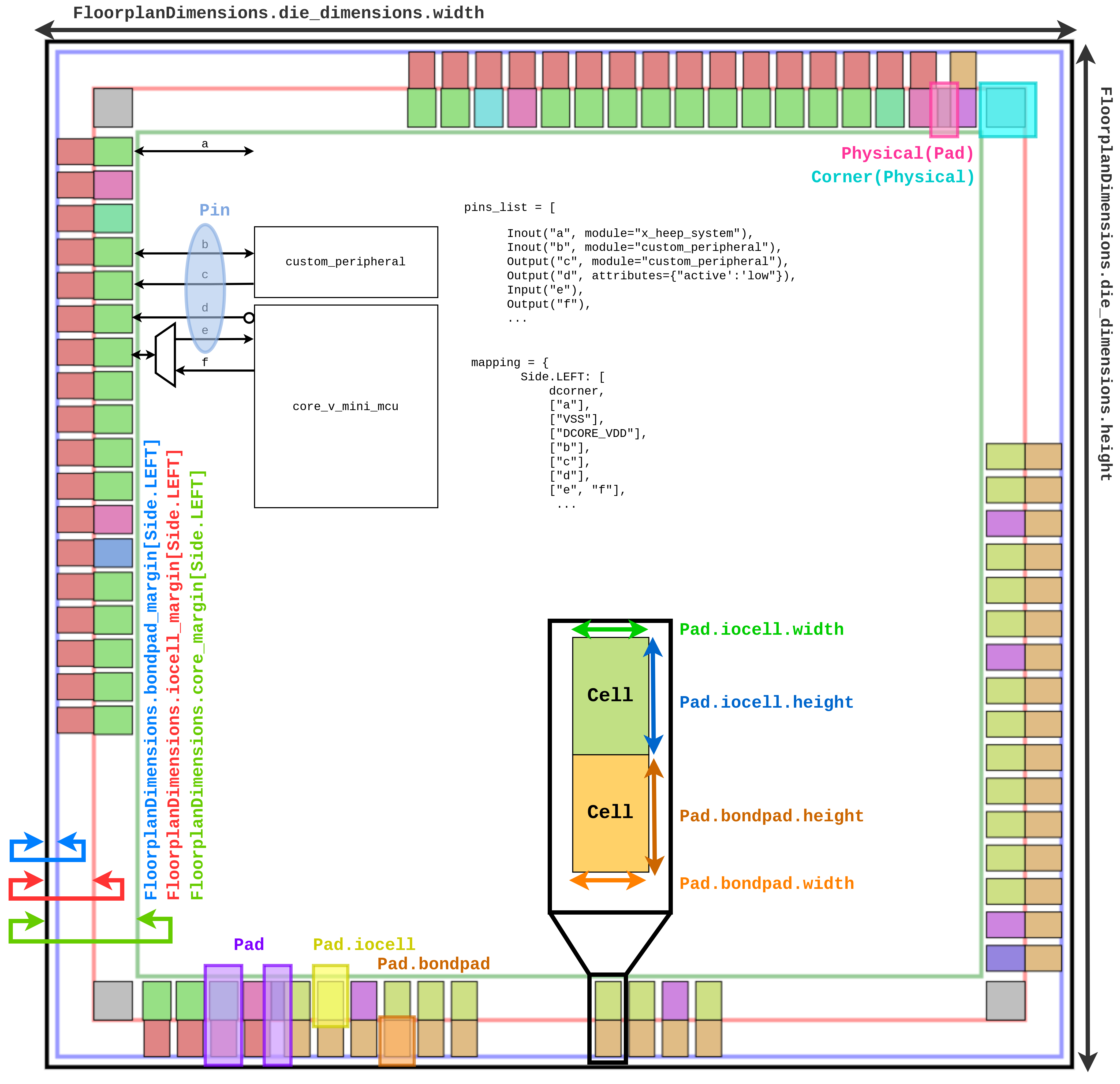 The base of the image above is an example of the diagram generated. References to the dimensions were added on top.
😎 X-pert Zone (mostly for ASIC implementation)
Custom Pad Attributes
You can add custom attributes to the PadRing for technology-specific features:
padring = PadRing(
    floorplan_dimensions=None,
    pin_list=list(pin_dict.values()),
    mapping=mapping,
    attributes={
        "bits": "7:0",  # Custom bit width for pad control
        "resval": 0x0,  # Default reset value for pad control
        "technology": "sky130",
    },
)
These attributes are accessible in template files during RTL generation. The following predefined attributes are supported for pad control generation:
bits: Bit range string that defines the pad attribute field width (e.g.,"7:0"or"3:0").resval: Reset value for the pad attribute register. Must fit in the width defined bybits.constant_attribute: Per-pad attribute (set on a Pad/Pin attributes dict) that, whenTrue, fixes the pad attribute toresvaland omits the writable register for that pad.
Example:
# PadRing attributes
padring = PadRing(
    # ...existing args...
    attributes={
        "bits": "3:0",
        "resval": 0x5,
    },
)

# Per-pin/per-pad attribute to lock the pad attribute
gpio = Inout("gpio_0", attributes={"constant_attribute": True})
Spacing Pads by Pitch
For precise physical placement:
# After creating the padring
padring.space_side_by_pitch(
    side=Side.TOP,
    space_from_corner_cell=100.0,  # µm from corner
    pitch=50.0,  # µm between pads
)
You can optionally space any pad from the edge by forcing the iocell_center_to_ring_edge attribute.
padring.pad_list[31].iocell_center_to_ring_edge = 1000
Custom pads cells
You can add customs cells that you need on your cheep according to the properties on the PDK.
# Update a cell defined in pin.py
cell.iocell_a.update( dimension=Dimension(width=60, height=65), name="PADIOA" )
# Create custom cells as defined by the PDK
iocell_dVdd = Cell( width=65, height=65, name="PADVDDIO",   rtl_wrapper="pad_cell_digital_core_vdd",  connections=["vdd"] )
For new cells, remember to also create an RTL wrapper and name them consistently (check those in hw/simulation).
Custom Pin types
Once you have custom pad cells, you can assign them to your custom Pin types:
class DVdd(PinSupply):
    """
    Represents a digital Vdd supply pin.
    """

    def __init__(self, name, attributes=None):
        super().__init__(name, attributes)
        self.iocell = iocell_dVdd.copy()
        self.bondpad = bondpad_d.copy()
Then you can add pins to your pad ring using these custom Pin types as you would with the standard ones from X-HEEP.